


Research in materials science drives innovation in application areas including, but not limited to: batteries, catalysts, drug delivery, space exploration, infrastructure and transports. Material science therefore addresses a breadth of global challenges from energy and environment to healthcare and beyond.
Characterisation – Atomic Force Microscopy & Imaging Spectroscopic Ellipsometry
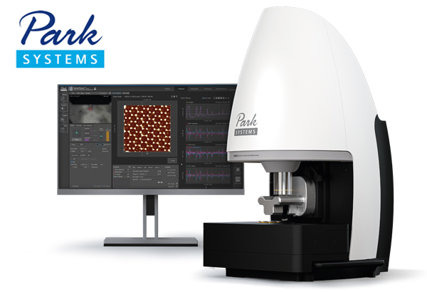
Atomic Force Microscopy is a crucial tool in materials science for characterising surface properties at the nanoscale. With the highest resolution, AFM will offer topographical detail, mechanical properties and functional information due to its various modes of operation. Examples of materials such as perovskites used in photovoltaic cells, QLED’s used in displays, polymers developed for contact lenses, metals and ceramics, and 2-D materials like graphene with its un-paralleled qualities, are just some of the real world examples of materials developed via the application of AFM.
Quantum Physics is also where AFM is likely to support key developments of quantum devices and systems, with unique modes like KPFM****
Latest developments from Park in Imaging Ellipsometers allow characterisation of thickness and refractive index on micro-structures as small as 1 um. With ellipsometric-contrast live-view, sub-nm features are detectable facilitating 3D maps of thickness (0.1 nm – 10 um) and refractive index.
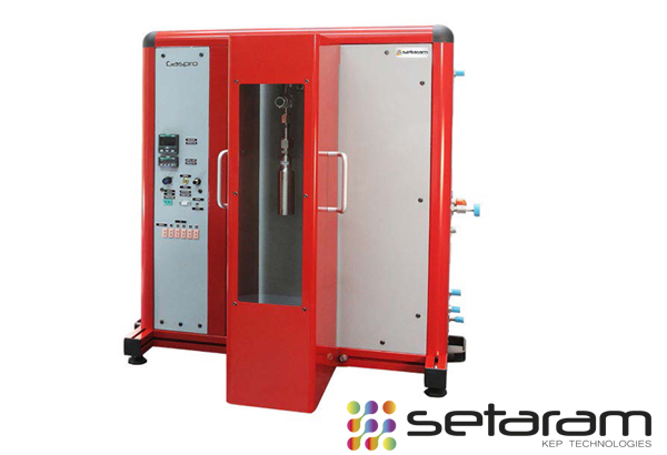
Characterisation – Thermal Analysis
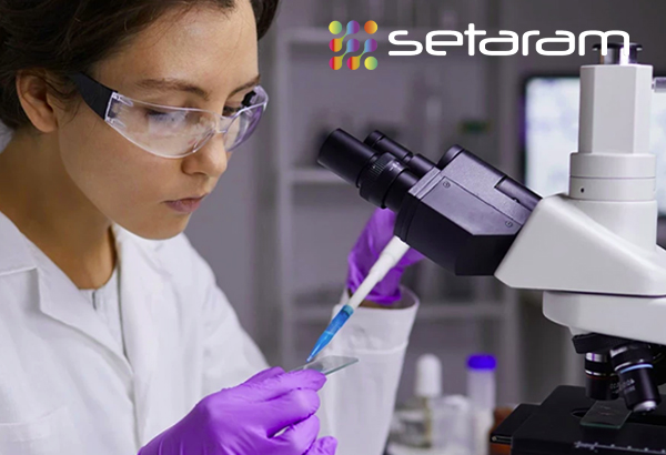
The structure, properties, and reactivity of every material- no exception- changes with temperature. Systems from Setaram have a true home in every material science research or industrial laboratory. Techniques like Differential Thermal Analysis (DTA), Simultaneous Thermal Analysis (STA) and Thermo Gravimetric Analysis (TGA) are deployed to determine the temperature and heat of reactions, glass transition and phase changes (i.e. melting, crystallisation), drying desorption and more.
TGA and STA can also measure mass variation during materials transformation during its catching or releasing of gases and can be combined with heat and temperature measurements. Typical studies include solid-gas reactions (i.e. oxidation, reduction), thermal stability (i.e. decomposition) or Compositional Analysis to determine material contents. Thermo Mechanical Analysis (TMA) instruments are designed for analysis of dimensional variation of materials when heated. For thermal expansion, softening or sintering measurements.
Characterisation – Calorimetry
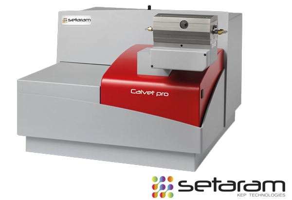
Differential Scanning Calorimetry (DSC) is an essential tool in materials science research, offering detailed insights into the thermal properties and behaviour of materials. Its applications range from studying phase transitions and thermal stability to characterising polymers, composites, pharmaceuticals and biomaterials. With its high sensitivity and quantitative capabilities, providing accurate measurement of Heat, Heat Flow and Heat Capacity which informs the development, optimisation, and application of materials across various scientific and industrial fields. Our CALVET calorimeters provide the most accurate calorimetry measurements- designed to be versatile by offering many interchangeable options such as mixing, circulation, high pressure, drop measurement or coupling to other instruments.
Characterisation – Gas & Vapour Sorption
Adsorption measurement and analysis with GASPRO is a fully automated solution for high pressure gas sorption measurements and analysis of materials. It is ideally suited to Energy & Environment applications like hydrogen storage, CO2 capture and sequestration, sorption onto geological substrates, and other porous solid characterisation. Our systems employ Sievert’s manometry method, which consists of injecting gas doses of increasing pressure on a sample and measuring the pressure change – Absorption, Adsorption and Desorption can be characterised. There are differing sample holders available that accommodates testing from vacuum to 200 bar, through temperature ranges of sub ambient to 500 oC.
Material Deposition – Slot-die Coating
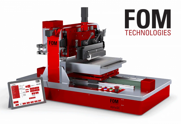
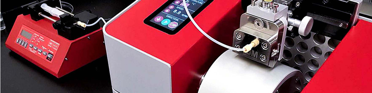
Slot-die coating is a highly scalable technique for rapidly depositing thin and uniform films with minimal material waste and low operational cost. FOM offer sheet based, roll based and roll-to-roll based machines that can deposit uniform dry films from nanometers to microns in thickness. Slot-die coating technology is usable to coat materials such as glass, metal, and polymers. This is achieved by precisely metering the process fluid; dispensing it at a controlled rate while the coating die is moved relative to the substrate. FOM Technologies specialise in machines and equipment for slot-die coating of functional materials. Application areas include but are not limited to development of advanced battery chemistries and architectures, development of next generation PV technologies via roll-to-roll and sheet-to-sheet techniques, and Power-to-X technologies.
Material Deposition – Physical Vapour Deposition (PVD)
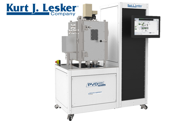
Physical Vapour Deposition, or PVD, involved the physical transfer of material from a source to a substrate – typically vaporisation of a solid, or liquid source material, which then condenses onto a substrate to form a thin film. Kurt J Lesker provide the material science market with highly versatile and broadly applicable range of Physical Vapour Deposition (PVD) Thin Film Solutions, also encompassing Chemical Vapour Deposition (CVD) and Atomic Layer Deposition (ALD). With hundreds of systems in use worldwide, they will accommodate many configurations with either glove box integration, load lock; and furthermore, can combine multiple techniques like e-beam, low-temperature evaporation (LTE) sources, thermal evaporation and magnetron sputtering sources. Systems are in use in applications from wear-resistance to data storage, decorative coatings to optics and display technologies, superconductors to semi-conductors, and fundamental physics research, in for example nanotechnology and spintronics that leverages the quantum mechanical property of electron spin to enhance functionality and performance.
Material Deposition – Plasma Enhanced Chemical Vapour Deposition (PECVD)
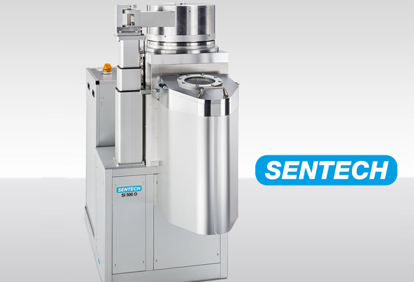
Plasma Enhanced Chemical Vapour Deposition (PECVD) is a type of advanced CVD technique that uses plasma to enhance the process of creating a thin film from a gas or vapour onto a substrate. Sentech offers systems offers system that produce films of excellent conformality and compositional uniformity, even at low temperatures. Critical applications where PECVD will be widely deployed include MEMS and NEMS, Solar Cells, Optoelectronics (i.e. transparent conductive films and optical coatings), and semiconductor industry for depositing insulating layers (dielectrics) or passivation layers (protective coatings).
ICPECVD, similar to PECVD which deploys an Inductively Coupled Plasma (ICP) source that generates a high-density plasma, enhancing ionisation of precursor gases that can lead to improved quality and uniformity of the deposited films. Additionally, the films are generated at lower temperature and with enhanced deposition rates making it more efficient in many applications, examples including when coating complex geometries and high aspect ratio structures.
Sentech combine into their portfolio further deposition systems including Atomic Layer Deposition (ALD), which are characterised by atomic-scale thickness control in applications requiring nanometer-level accuracy and precision. It is now indispensable for advanced technologies development as it can be considered scalable and able to be integrated with other processes during deposition and fabrication. With Sentech you will expect ultra-thin pinhole and particle-free films. Simplified by the implementation of the Sentech AL Real Time Monitor, an optical diagnostic tool which facilities development of and optimisation of atomic layer processes. Monitoring adsorption and desorption with ultra-high 40 ms time resolution with sub-angstrom thickness resolution.
Material Cleaning & Activation
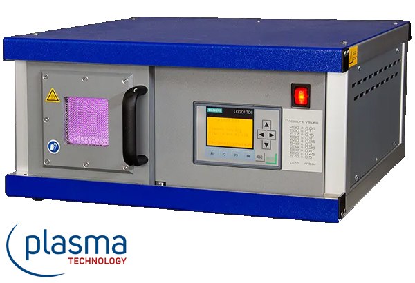
The use of plasma to optimise material surfaces has long been a technical standard in industry. In physics, plasma is often described as an ionised gas consisting of negatively charged free electrons and positively charged ions and neutral particles. Material properties during treatment are specifically changed by choosing the gas composition (typically air, nitrogen, or oxygen) and the type of energy coupling, typically DC, kHz, MHz (radio frequency) or GHz (microwave frequency).
Cleaning to remove grease, oils, waxes, and other organic and inorganic contamination (also oxide layers) is essential for materials to undergo further processing such as sputtering, PVD and CVD coating, printing, bonding, soldering etc.
During plasma activation, functional groups are generated to improve the surface to which paint systems or adhesive systems ae applicable. By means of etching or plasma structuring, the reactive species of the plasma removes material from the surface, and the resulting microstructure creating a larger surface area.
Our portfolio of plasma systems range from 2L to 40L benchtop systems for laboratories or small production environments. Devices feature built-in microcontrollers or industrial PC so that recipes can be created and parameters are controlled to enhance process reproducibility. For larger samples or larger production processes, we can offer bespoke plasma systems engineered for 24/7 operation and can also include automation.
Material Modification / Etching – Plasma Etching
Plasma etching in material science is relevant to very selectively modify and create surfaces at the micro and nanoscale. Reactive Ion Etching (RIE) is a combination of physical and chemical etching, where ions bombard the surface to create damage sites that are more reactive to the chemical etchant. Systems from Sentech deploy Inductively Coupled Plasma (ICP) source with low ion energy for low-damage etch and nanostructuring. Additionally, Sentech have developed a proprietary plasma source technology – Planar Triple Spiral Antenna- which is a unique and high-end feature that offers uniformity and high ion density, low ion-energy suited to applications of sensors, quantum dots, and HEMT. Substrate temperature management during the plasma etching processes are demanding criteria for high-quality etching. The substrate electrode with dynamic temperature control in combination with helium backside cooling and substrate backside temperature sensing facilitates extreme confidence and control in every process.
Sentech offer flexible and modular design, with optimised configurations for processing a variety of materials including III-V and II-VI compound semiconductors, dielectrics, quartz, glass, silicon, silicon compounds and metals.
Material Preparation and Processing – Temperature Control
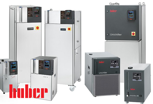
Since the past 50 years, Huber temperature control unit have revolutionised the world of temperature control technology. In research and industry, Huber’s high precision temperature control solutions span a product range in the field of liquid temperature control of material tests from -125 to 425 C. Industries we serve range from Chemicals and Pharmaceuticals, Botanical Extraction, and Biotechnology, through to Automotive, Space/Aerospace and Semiconductor/Electronics. While testing under differing environmental conditions is a major application, equally sought after are our highly accurate systems during materials processing or manufacturing. Precise and reproducible temperatures are crucial and include complementing the instrumentation shown within this webpage. Applications include (but not limited to) degradation under thermal influences, controlling endothermic or exothermic reactions, controlling phase transitions or simply put – offering efficient heat transfer or cooling affect.
Material Preparation and Processing – Gloveboxes, Solvent Purifiers & Gas Purifiers
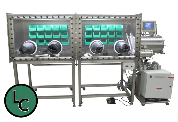
LC Technology Solutions design, build and supply the highest quality bespoke custom gloveboxes, solvent purifiers and laboratory high pressure gas purifiers. For more basic requirements we offer solutions from our partner Etelux. Gloveboxes are an indispensable tool in materials preparation and processing due to their ability to create a controlled, oxygen- and moisture-free environment. They are essential for handling air-sensitive materials, performing reactions that require inert conditions and ensuring the purity and stability of sensitive compounds. For example, energy storage has the potential to transform the global economy. Lithium metal and lithium salts are highly reactive with air and moisture and are just an example of some important materials used in Lithium-Ion batteries, and our gloveboxes are essential for the assembly of battery cells and the preparation of electrode materials to ensure contamination and degradation are minimised. Their use is far more widespread in research and production of nanomaterials, thin films, semiconductors and more – covering some of the most advanced materials at the forefront of technology.
Material Preparation and Processing – Mass Flow Controllers & Meters
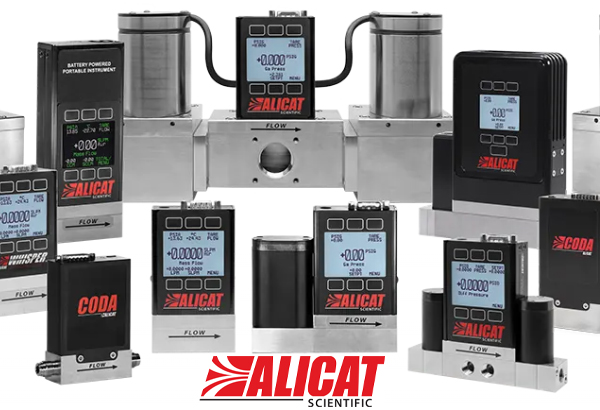
Alicat Scientific manufacture custom mass flow and pressure meters and controllers for gas and liquid applications. Within the gas flow and measurement and control portfolio, are their famous pressure based instruments with incredible accuracy, have no warm-up time, fastest millisecond response times for lightning-fast control, and multi-gas compatibility. Models ranges will provide high performance for most applications from 0.5 SCCM of flow all the way up to 10,000 SLPM, and with pressure ranges from less than 1 PSI all the way up to 4000 PSIA. Industries which Alicat instrumentation are in use include aerospace/defence, food and beverage, glass and optical fibre, hydrogen, biopharma, nanotechnology and nanofabrication. During thin film deposition, production of thin film coatings requires fast, and precise gas delivery into vacuum coating systems. Another emerging application is within the new Hydrogen economy. Tailored solutions for regulating mass flow and pressure have the potential to overcome obstacles within the hydrogen industry. From direct regulation of electrolysis and fuel cell system processes, to test benches for membrane and catalyst verification, Alicat offers countless flow and pressure solutions so you can focus on creating a more sustainable future.
Material Preparation and Processing – Chemistry Equipment
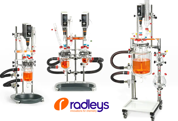
Radleys provide innovative chemistry equipment for safer, cleaner, greener and more productive chemical research, development and production – with a focus on chemical synthesis and process development. With glassblowing production facilities operating since the 60’s, critical to materials processes are glass jacketed reactors. In essence their ability to offer temperature control, mixing, adaptation to different material types, safety and overall process control and ultimately scalability is reason why it is an indispensable tool for synthesis, research, testing and production of advanced materials. Typical materials processing applications include the synthesis of polymers, nanomaterials, and composites. With AVA software in control, scalable production of materials with specific properties is made easy.
Material Preparation and Processing – Freeze Drying
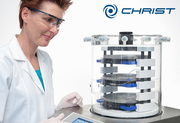
In most material science research facilities in our region, you will find a freeze dryer in use, and usually it’s a Martin Christ that was supplied by Scitek. Martin Christ is the world leader in the development and manufacture of freeze dryers, with over 75 years of experience. It is the only manufacturer in the world that provides systems that range from small 2 kg desktop laboratory research units, through to 6-20 kg pilot scale systems with patented and advanced Process Analytic Tools, through to production scale machines from 20 to 500 kg and more.
Freeze dryers (also termed lyophilisers) will serve multiple functions in material science and engineering due to their ability to remove solvents (like water) without causing thermal degradation, directly manipulating and preserving material properties, and can better maintain the material structure, stability and purity throughout the process as compared to alternative techniques. The removal of solvent from the sample (that occurs during the physical phenomenon of sublimation) is the fundamental generic application of material processing. In addition to this, and when subsequently handled correctly, freeze drying will enhance the stability and shelf life of sensitive materials. Traditionally biotechnology and biopharma laboratories are typically where our freeze dryers can be found in batch type processes. However, other popular applications for material preparation include (a) creating highly porous structures like developing aerogels and foams used in catalysis, filtration, and insulation, (b) making nanomaterials and nanocomposites, and (c) drying of hydrogels to maintain their network structure and porosity, for developing drug delivery systems or tissue engineering.
Potential Free Atmospheric Plasma
Atmospheric plasma is commonly used in industrial and manufacturing settings for surface treatment, surface cleaning and surface activation – often as preparation step for bonding or coating applications. Different types of atmospheric plasma have varying effects based on electrode types, electrode materials, plasma frequency, gas, plasma temperatures and much more. Our solutions range from small experimental systems for research to large area solutions that can be integrated into industrial automation and robotics.
Solar Simulators
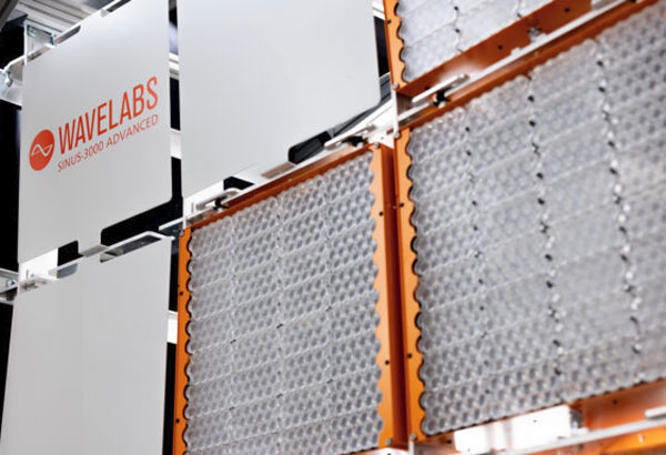
LED solar simulators support photovoltaic research, production and metrology. They simulate sun light for non-destructive testing of cells and entire assembled modules. The key in solar simulation is the high precision replication of the sun’s spectrum just as much as high accuracy isolation of specific wavelengths. Wavelab’s LED technology does that like no other. Applications for solar simulations go far beyond photovoltaics and include semiconductors, UV curing and exposure, life sciences and even horticulture.