
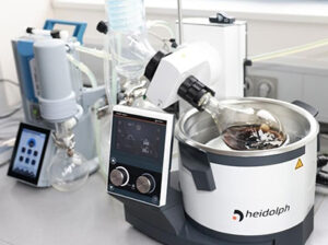
Material Science
Research in materials science drives innovation in application areas including, but not limited to: batteries, catalysts, drug delivery, space exploration, infrastructure and transports. Material science therefore addresses a breadth of global challenges from energy and environment to healthcare and beyond.
read more
Analytical Instrumentation
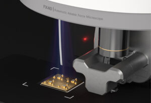
Electron Spectroscopy refers to a group of techniques used to analyse the energy distributions of electrons emitted from or scattered by a sample. In 1983, two years after receiving the Nobel Prize – Professor Kai Siegbahn co-founded Scienta for the continued development of electron spectrometers and systems.
read more
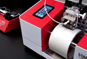
Food and Beverage

The use of vacuum facilitating processing technology in food production, quality control and new food development is growing quickly. Scitek technologies add value through preservation, weight reduction, shelf-life extension and extraction of actives.
Nanofabrication
Scitek has comprehensive capabilities in nanofabrication, excelling in precision manufacturing at the nanoscale. Their expertise encompasses advanced techniques like electron beam lithography, thin film coatings, atomic layer deposition and reactive ion etching
read more
Service and Maintenance
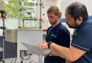
How much will it cost you if your equipment stopped working tomorrow? Whether you are in research or in production, your equipment is critical to your success and maintenance is an important
read more
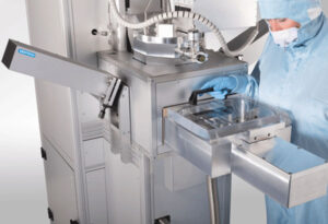
Pharmaceutical Science

For the Pharmaceutical Science Industry, Scitek offers instrumentation and equipment solutions (and services) that are able to assist you in conducting of research and development, from the scientific laboratory and
read more
Custom Engineering

At Scitek, customization is at the heart of what we do. Whether you require intricate PLC designs, seamless integration of vacuum systems, or innovative engineering solutions to overcome technical hurdles, we possess the knowledge and capabilities to deliver. read more
Industrial
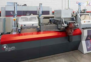
At Scitek we can cater to your manufacturing needs, ranging from sample preparation for coating processes to metallisation and deposition procedures for the semiconductor, solar, battery, automotive, battery and decorative industry.
read more