


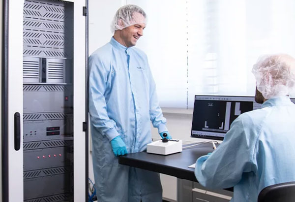
Scitek has comprehensive capabilities in nanofabrication, excelling in precision manufacturing at the nanoscale. Their expertise encompasses advanced techniques like electron beam lithography, thin film coatings, atomic layer deposition and reactive ion etching. These technologies enable the creation of intricate nanostructures and devices with exceptional precision. Scitek’s nanofabrication proficiency caters to various sectors, including electronics, photonics, and materials research, driving innovation in micro- and nano-scale components.
Slot Die Coating
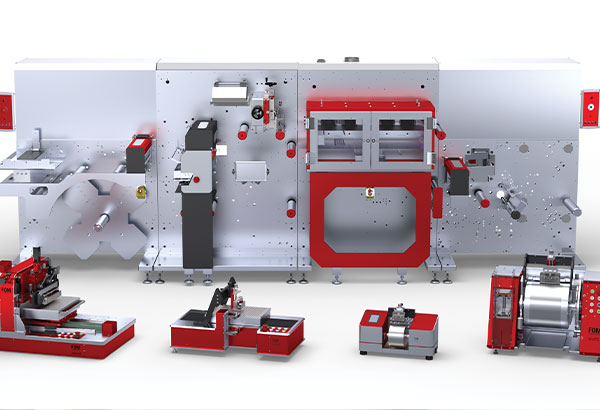
Slot die coating is a precise method used to apply thin liquid films uniformly onto surfaces. It involves liquid passing through a narrow slot and spreading smoothly onto a substrate. The key principle involves regulating the liquid flow rate and slot-to-substrate distance to achieve consistent coating thickness. FOM Technologies specializes in slot die coating solutions, offering advanced equipment for research and industry needs. Their technology ensures controlled and efficient coating processes, crucial for various applications. By providing reliable coating solutions, FOM contributes to improved product quality and innovation in industries ranging from electronics to energy.
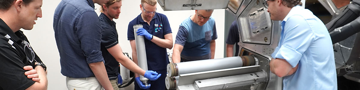
Roll to Roll Coating
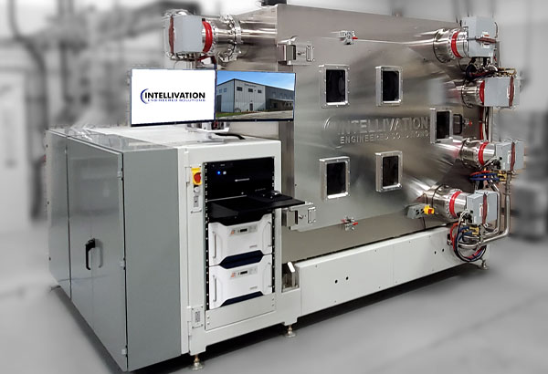
Roll-to-roll (R2R) coating is a continuous process for applying thin films to flexible substrates like rolls of plastic or metal. It involves feeding a substrate through a series of coating, drying, and curing steps, enabling high-speed and cost-effective production. The fundamental principle relies on precise control of coating materials, speeds, and environmental conditions to achieve uniformity. Intellivation specializes in R2R solutions, offering advanced technologies for applications like printed electronics. Their expertise ensures consistent and efficient coating processes, enhancing productivity in industries requiring large-scale and flexible material coatings. R2R coating revolutionizes manufacturing by enabling the production of flexible electronics, solar cells, and more.
FOM Technologies also specialise in R2R platforms, but targeted at liquid deposition, as opposed to metal evaporation or sputtering technologies. Their applications are endless and enable rapid prototyping and pilot manufacturing in applications such as batteries, supercapacitors, Medtech and pharma, fuel cell, electrolysers, carbon capture, DAC and defence.
Their range varies from a compact versatile R2R slot die coater, with its modular design and multiple drying options enabling flexibility in the evolving research needs to a highly capable, modular roll to roll pilot line platform.
Electron & Ion Beam Lithography
Electron and ion beam lithography are advanced nanofabrication techniques used to create intricate patterns on surfaces at the nanometre scale. They involve directing focused beams of electrons or ions onto a substrate coated with a resist material. The fundamental principle is that these beams can accurately remove or modify the resist, allowing for precise pattern transfer onto the substrate. Raith specializes in electron and ion beam lithography solutions, providing cutting-edge systems for applications in research and industry. Their technology empowers researchers and engineers to create nanostructures with exceptional detail, advancing fields like microelectronics, photonics, and materials science.
Atomic Layer Deposition
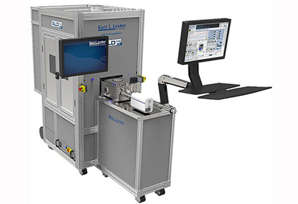
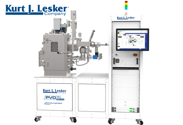
Atomic Layer Deposition (ALD) is a nanotechnology technique used to create thin and precisely controlled layers of material on surfaces. It involves alternating cycles of chemical reactions, where gaseous precursor molecules react with a substrate’s surface to form a layer one atomic or molecular layer at a time. This self-limiting process ensures excellent uniformity and conformality, even on complex 3D structures. SENTECH and Kurt J Lesker offer ALD solutions, allowing for precise material deposition in various industries like semiconductors and advanced coatings. ALD’s fundamental principle of layer-by-layer growth plays a pivotal role in enabling cutting-edge technologies and research applications.
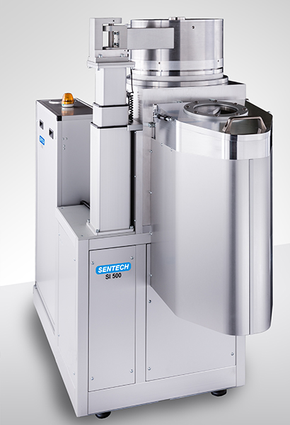
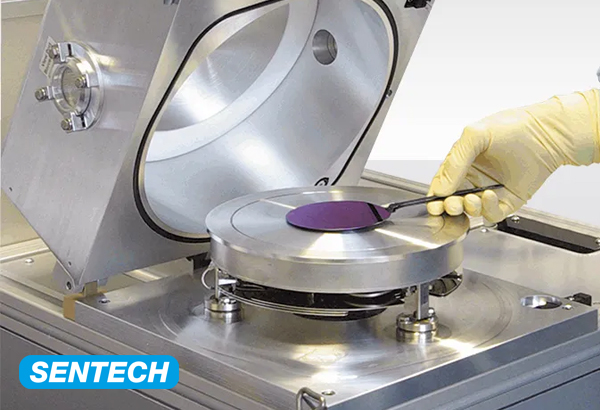
Reactive Ion Etching
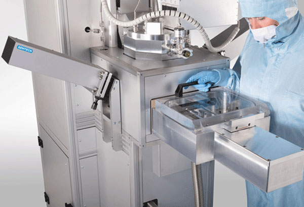
Reactive Ion Etching (RIE) is a process used for precision material removal in microfabrication. It involves a plasma, typically formed by reactive gases, which chemically reacts with the material’s surface and removes it. This etching is directional due to the ion bombardment from the plasma, resulting in controlled material removal. SENTECH specializes in RIE solutions, offering advanced equipment for surface modification. The fundamental principle of RIE involves the chemical and physical interactions between the plasma and the material, enabling controlled etching with applications in microelectronics, optics, and sensor fabrication, providing high-precision material shaping and patterning capabilities.
Thermal Evaporation
Material is heated in a vacuum until it vaporizes and then condenses onto a substrate to form a thin film. This technique is suitable for materials with low melting points and is used for optical coatings, thin film transistors, and in the fabrication of various electronic components.
Electron Beam Evaporation
A more advanced method that uses a focused electron beam to heat and evaporate materials with high melting points. This technique offers precise control over the deposition rate and material composition, making it suitable for complex layered structures. It is particularly beneficial for applications in microelectronics and photonics. Commonly used for the deposition of metals, dielectrics, and complex alloys; electron beam evaporation provides high-quality films with excellent uniformity. These systems are designed to minimize contamination, which is crucial for applications requiring high material purity where deposition can be performed in high-vacuum environment.
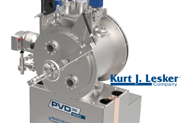
Sputtering
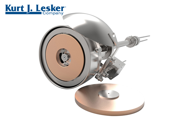
A target material is bombarded by ionized gas, causing atoms to eject and deposit on a substrate. It includes variants like DC, RF, and Magnetron sputtering, which are commonly used for high-quality, uniform coatings in electronics and industrial applications. This method is highly versatile and can deposit a wide range of materials, including metals, oxides, and nitrides.
Kurt Lesker’s sputtering systems are designed for high performance and scalability. They can be configured for single or multiple targets, enabling users to create complex multilayer films. Modular systems can be tailored to specific research or production needs, accommodating various substrate sizes and materials. Users benefit from advanced control sophisticated eKlipse software for real-time monitoring and control of the deposition process, enhancing repeatability and accuracy.
Inductively Coupled Plasma Reactive Ion Etching (ICP-RIE)
This is an advanced etching technique used in microfabrication, providing highly anisotropic and precise etching. Unlike traditional reactive ion etching, ICP-RIE uses an inductively coupled plasma source to generate a high-density plasma independently of the electric field that accelerates ions towards the substrate. This separation allows for greater control over ion density and energy, enabling deep and high-aspect-ratio etching while minimizing surface damage. ICP-RIE is widely used for complex etching applications in semiconductor manufacturing, such as creating deep trenches and detailed patterns in silicon and other materials for MEMS and advanced electronic devices.
Plasma-Enhanced Chemical Vapor Deposition (PECVD)
PECVD utilizes plasma to enhance the deposition process, allowing for low-temperature film growth. This method is particularly effective for materials like silicon dioxide and silicon nitride, which are essential in electronics and optics. PECVD offers excellent step coverage and uniformity, making it suitable for complex substrates. CVD is also used for depositing various metal oxides used in materials science.
Spin Coating
Spin coating is a widely used technique in lithography for preparing thin, uniform films on substrates. The process involves several key steps including Substrate Preparation, Material Application, Spinning and Drying. Key Benefits include high levels of uniformity, process control and scalability.