SEM Sample Preparation
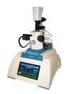
PEC II System
Broad argon ion beam system designed to polish and coat samples for SEM imaging and analytical techniques.
PEC II System - Advantages
Fully automated argon ion polishing system suitable for preparation of SEM samples to prepare damage free surfaces, cross sections and deposit coatings to protect or eliminate charging.
- Polish, etch or coat samples with a single pump down
- Etch at voltages as low as 100 V for rapid and damage free preparation of sample surfaces
- Permit samples as large as 32 mm in diameter
- Transfer samples from the PECS™ II instrument to a SEM/FIB or glovebox without exposure to air (optional)
- Store and analyze image in DigitalMicrograph® software from Gatan for digital optical imaging
- Display and control all PECS II parameters using integrated 10-inch color touch screen
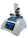
Ilion II System
Ideal for low energy surface preparation for your SEM cross section viewing.
Ilion II System - Advantages
- Vacuum load-lock and liquid nitrogen cold stage to provide rapid workflows on beam sensitive samples
- Real-time observation of the polishing process including an optical microscope with digital imaging; images can be stored and analyzed with DigitalMicrograph® software from Gatan
- Repeatable results from recipes and operation of the Ilion™ II via a 10" color touch screen interface
- Damage-free surfaces for analytical techniques, such as cathodoluminescence and EBSD, where the signal is generated near the surface
SEM Specimen Stages

Murano and Microtest In-Situ Stages
A range of heating and tensile stages specifically designed to enable your in-situ research.
Murano and Microtest In-Situ Stages - Advantages
In-situ heating and tensile testing stages allow dynamic microstructural observations and can provide new insights into materials research.
- Modules are specially engineered for the scanning electron microscope (SEM) environment
- Custom designs allow quick fitting and removal from SEM stages so normal SEM use can be resumed quickly
- Designed to be compatible with geometrical requirements of different detectors including electron backscatter diffraction (EBSD) for dynamic observations
Heating stage modules
- Murano stage available for heating to 950 °C for EBSD applications and secondary electron detector (SED) imaging
- Study real-time crystallization and phase transformations at elevated temperatures up to 950 °C
- Proprietary design enables offline specimen mounting and storage
- Bulk specimen support designed specifically to operate within EBSD/focused ion beam (FIB)/SED geometry constraints
- Water cooling and heat protective shielding ensure maximum protection at elevated temperatures
- Additional bias control to assist with imaging at elevated temperatures
Microtest tensile stages
- Allows dynamic testing experiments in the SEM
- Provides a deeper understanding into what causes the deformation; and the ability to image where the microstructure change is occurring
- Tensile, compression and bending tests available
- Options for different load cells with load ranges from 2 N up to 5000 N to provide greater resolution for a wider range of specimens
- Easy to use software interface provides live graphing of quantitative data together with flexible thresholding for more complex experiments, including cyclical loading
- Unique MTVideo option allows synchronized image and data acquisition providing detailed post experiment analysis of the sample deformation and corresponding captured SED images
- Option for complete replacement X,Y,Z stage door for SEM provides greater flexibility for heavier stages
| Model # | Maximum tensile load | Heating option | Cooling option | EBSD option | 3 or 4 Point bending option | Changeable load cell |
|---|---|---|---|---|---|---|
| Mtest200 | 200 N | √ | √ | √ | √ | |
| Mtest300 | 300 N | √ | √ | |||
| Mtest2000 | 2000 N | √ | √ | |||
| Mtest2000E | 2000 N | √ | √ | √ | ||
| Mtest5000 | 5000 N | √ | √ | √* | √ | √ |
Cooling Stage
Helium and liquid nitrogen stages to monitor cryogenic or temperature dependent studies to better understand your electrical and electronic materials.
Cooling Stage - Advantages
- Beam sensitive materials are stabilized under high beam currents
- Low temperature phases can be studied
- Enhanced imaging and spectroscopy, especially for cathodoluminescence (CL)
| Model # | Base temperature | Cool down time | Maximum operating temperature | Tilt | Rotate | Additional electrical feed through option | |
|---|---|---|---|---|---|---|---|
| C1001 | -185 °C | 10 min | 50 °C | 45° | ±5° | √ | |
| C1002 | -185 °C | 10 min | 200 °C | 45° | ±5° | √ | |
| C1003 | -185 °C | 10 min | 400 °C | 45° | ±5° | √ | |
| CF302 | 6 K | 45 min | 140 K | √ | |||
| CF302M | 8 K | 55 min | 140 K | ±5° | √ | ||
Liquid nitrogen cooling stages C1001, C1002, C1003
- Simple installation/removal allows use of standard SEM stage
- Stages cooled to less than -185 °C by nitrogen gas
- Efficient thermal design ensures rapid cool down and stable temperatures
- Accurate control through integral heater and temperature sensor
- External liquid nitrogen heat exchanger removes vibration due to boiling of LN2
- Higher upper temperature options for more flexibility in experiments
Liquid helium cooling stages CF302, CF302M
- Specially designed low drift and vibration, while minimizing liquid helium consumption
- Complete replacement SEM stage and door assembly with X, Y, Z axis manual micrometers
- Faster sample exchange through compatibility with C1010 airlock loading system from Gatan
- CF302M is a helium-cooled stage module that attaches onto SEM goniometer, and requires more care than the CF302
- Complete system includes flexible transfer tube storage vessel, top fitting with bladder and valve, gas flow controller, gas flow pump, and digital temperature controller
- Optional radiation shield can be included depending on intended use and configuration
Dual fuel option
- Allows liquid helium cold stages to be operated with either helium or nitrogen
- Functions by forcing cold nitrogen gas through the circuit similar to successful C1002 product
Accessories—Anti-contaminators
- Accessories include C1005, C1006, or C1007 anti-contaminators
| Model # | Base temperature | Cool down time | Maximum operating temperature | Heater control | Individual cooling circuit |
|---|---|---|---|---|---|
| C1005 | Less than -185 °C | 10 min | 50 °C | ||
| C1005B | Less than -185 °C | 10 min | 50 °C | √ | |
| C1006 | Less than -185 °C | 10 min | 50 °C | √ | |
| C1007 | Less than -185 °C | 10 min | 50 °C | √ |
SEM Imaging & Spectroscopy
Serial Block-Face Imaging
3View System
Automate sectioning and image capture of your 3D ultra-structure using serial block-face scanning electron microscopy.
3View System - Advantages
The 3View® system allows high-throughput, high-resolution imaging of a wide variety of samples in 3D. 32k x 24k image support and high-performance stages allow fully automated high-speed imaging of many different types of samples.
- Serial block-face imaging minimizes errors and distortions found when using focus ion beam imaging or traditional serial section imaging
- Large format image support (32k x 24k) allows you to collect very large images to minimize the amount of time wasted waiting for stage motion when imaging very large regions
- <50 nm X, Y stage repeatability allows multi-region imaging without losing data due to imprecise stage motion
- 15 nm Z section thickness without the need to unblur multi-kV images
- High-performance OnPoint™ backscattered electron (BSE) detector allows high-speed imaging at low kV, without giving up image quality
Cathodoluminescence
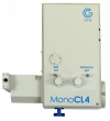
MonoCL4 System
World-leading catholuminescence imaging and spectroscopy system compatible with conventional, low vacuum or field emission SEM, combined FIB/SEM, and ion microscopes.
MonoCL4 System - Advantages
The MonoCL4™ system is the leading cathodoluminescence (CL) microscopy system for scanning electron microscopes (SEM) and electron probe microanalyzers (EPMA). Its supremely efficient collection and detection ensures the ultimate performance in sensitivity and spatial resolution from a wide range of bulk and nanoparticle samples.
- Reveal more than just morphology and compositional information
- Optical, electronic and crystal defect properties of semiconductors
- Phase and geochemical changes in rocks, minerals, and ceramics
- Surface plasmon (optical) properties of metallic nanostructures (plasmonics)
- Inter- and intra-molecular structure of organic materials
- Designed from the ground up for cathodoluminescence microscopy, seamlessly integrating into an electron microscopy environment, and compatible with all major brand SEM
- Ultimate sensitivity and spatial resolution across a broad range of wavelengths from deep UV to near infrared using achromatic collection optics with optimized collection efficiency and minimum optical losses using direct optical coupling
- Analyze sensitive or weakly emitting materials fast and with full confidence utilizing the highest efficiency panchromatic imaging mode (total light with spectral filtering, if required) and fast spectroscopy detector option
- Optimize hardware and software capabilities for specific applications with fully customizable and upgradeable basic instruments from Gatan
- Compatible with Gatan’s range of cryogenic stages and SmartEBIC products
| MonoCL4 | Swift | Plus | Elite | |
|---|---|---|---|---|
| Cathodoluminescence imaging and spectroscopy | √ | √ | √ | √ |
| Panchromatic (total light) and spectrally resolved imaging modes | √ | √ | √ | √ |
| High collection efficiency | √ | √ | √ | √ |
| Direct achromatic coupling (no optical fibers) | √ | √ | √ | √ |
| Instrument spectral resolution <0.5 nm | √ | √ | √ | √ |
| PMT for CL imaging and spectroscopy | √ | √ | √ | √ |
| CCD for fast spectroscopy | Optional | √ | Optional | √ |
| High performance PMT for imaging and spectroscopy | Optional | Optional | √ | √ |
| Spectrum-imaging (hyperspectral imaging) | Optional | Optional | Optional | √ |
| Infrared detector(s) | Optional | Optional | Optional | Optional |
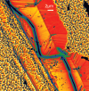
ChromaCL2 System
Live color cathodoluminescence imaging for your scanning electron microscope.
ChromaCL2 System - Advantages
The ChromaCL2™ system is a color cathodoluminescence imaging system for use in scanning electron microscopes (SEMs) and electron probe microanalyzers (EPMAs). The system is suitable for many petrographic and earth science applications where color cathodoluminescence imaging can reveal geochemical processes.
- Reveal macro- and micro-texture in sedimentary rocks including: sediment source, degree of compaction, diagenetic history, differentiation of authigenic and detrital minerals, cementation history, and provenance
- Simple operation
- Color cathodoluminescence images aid the interpretation of geochemistry changes
- Higher spatial resolution than bench-top flood gun systems
- Carbonate imaging kit to overcome phosphorescence from some carbonate minerals in scanned CL images
- Effectively unlimited field of view with field stitching software module
| Model | Color imaging (RGB) | UV sensitivity | Integrated back scattered electron detector | Field stitching software | Carbonate imaging kit |
|---|---|---|---|---|---|
| ChromaCL2 | √ | √ | Optional | Optional | |
| ChromaCL2UV | √ | √ | Optional | Optional | |
| ChromaCL2 iBSED | √ | √ | Optional | Optional | |
| ChromaCL2UV iBSED | √ | √ | √ | Optional | Optional |
MiniCL System
Cathodoluminescence imaging compatible with all scanning electron microscopes or microprobes.
MiniCL System - Advantages
Simple to use cathodoluminescence imaging system for use in scanning electron microscopes (SEM) and electron probe microanalyzers (EPMA). The MiniCL™ system is sensitive to luminescence from most geological specimens, and the detector is positioned close to the specimen boosting detection efficiency.
- Sensitive to ultraviolet, visible and near infrared wavelengths enabling panchromatic cathodoluminescence imaging of a wide range of minerals, ceramics, and LED materials
- Cathodoluminescence images at a spatial resolution higher than bench-top flood gun systems
- Use at all SEM magnifications to reveal macro- and micro-texture in sedimentary rocks including: sediment source, degree of compaction, diagenetic history, differentiation of authigenic and detrital minerals, cementation history, and provenance
- Convenient use with other SEM detectors including: secondary and backscattered electron detectors and energy or wavelength dispersive X-ray detectors
SEM Detector & Control
DigiScan II System
Digital beam control and image processing to enhance the photographic quality of your digital images.
DigiScan II System - Advantages
The DigiScan™ II system functions under the powerful DigitalMicrograph® software platform providing easy to use, yet flexible image acquisition controls, excellent signal-to-noise extraction techniques, and options for simultaneous acquisitions from multiple channels.
- Connects to nearly all SEM and STEM systems and provides a universal interface
- Optimize the image to fit the experiment—never compromise quality when using flexible scan and digitization
- Low noise and high-speed imaging utilizing differential analog-to-digital or digital-to-analog converter
- Simultaneous multiple signal acquisition and unique contrast modes
- Up to 4 analog and 4 pulse inputs simultaneously
- User choice of pixel image size in X and Y dimensions, up to 8192 wide x 8192 high
- Digitization at 1, 2, or 4 bytes per pixel
- User choice of pixel dwell time from 400 ns to 400 msec per pixel
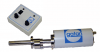
SmartEBIC System
Characterize the electrical properties of your semiconductor materials and devices.
SmartEBIC System - Advantages
- Quantitatively characterize electrical properties of materials and devices including: in-situIV tracing, identify p-n junction position and measure depletion region widths, determine minority carrier diffusion lengths and defect recombination strengths
- Designed for low noise DC measurement allowing picoamp accuracy current measurements
- Complete system from sample holder and specimen contacting to acquisition and analysis software
- Simple yet powerful software for experiment control and data analysis including auto set up routines

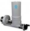
OnPoint BSE Detector
A back-scattered electron detector for high speed low kV imaging in the SEM
OnPoint BSE Detector - Advantages
Introducing the OnPoint™ detector, the new standard for backscattered electron (BSE) detection that delivers unprecedented sensitivity and speed to better understand nonconductive samples; such as polymers, plastics, and biological materials. Using a detector optimized for low kV, this system expands your ability to study uncoated biological samples, low atomic number (Z) elements, and large 3D datasets.
- Resolves features distorted by charging or beam damage: Attains images at low kV to reduce charge build-up and to prevent damage to delicate samples
- Captures large, 3D datasets quickly: Acquires large field of view images or 3D datasets up to six-times faster
- Differentiates low-Z elements: Delivers the highest signal-to-noise ratio (SNR) available to help differentiate between elements with a similar atomic number
- Provides highest BSE collection efficiency: Produces higher SNR images because it captures electrons other detectors miss as well as minimizes the noise in the detection system
- Ensures peak performance within minutes: Allows you to maintain your system at the highest performance without a service visit
SEM Analysis
3D Visualization Software
Explore your 3D data with volume rendering, isosurface, ortho slices and more.