Thin Film Technology

Courtesy of our historical involvement with Balzers thin film technology we have always been closely involved in coating technology.

Today Scitek continues to be your local coating technology expert with solutions ranging from research to industrial production, optics and media.

Whatever you are considering thermal evaporation, e-beam evaporation, sputtering, physical vapour deposition, plasma enhanced physical vapour deposition, etching, atomic layer deposition and many others – Scitek will have a solution for you.

Applications include basic thin film coating for electron microscopy preparation, semiconductor, optical coatings all the way to solar cell production.

Look no further than Scitek for;- Batch deposition in research- In-line coating for industrial production- Roll-to-roll coating in pilot and production

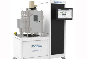
Kurt J. Lesker

Lesker offers their customers the advantage of unparalleled knowledge and expertise in the manufacturing of thin film vacuum deposition systems by staying on the leading edge of engineering and technology.

KJLC offers single-chamber deposition systems or cluster tools with robotic transfer for production and research applications, as well as extensive knowledge of process, application, mechanical, electrical, and software engineering – this is a powerful combination that keeps their customers one step ahead of their competition.

Thin Film Deposition Techniques and Capabilities

Methods used to deposit thin films are generally split into two categories: Physical Vapor Deposition (PVD) and Chemical Vapor Deposition (CVD), depending on the underlying principles causing film deposition. A PVD method evaporates or sputters a material, producing a gaseous plume or beam that deposits a film on the substrate.

A CVD method uses reactive, volatile compounds that decompose on a heated substrate. The starting materials are often organo- or hydrido-compounds that pyrolyse at relatively low temperatures into a non-volatile (film) component and a residual vapor/gas that is pumped out of the system. Both methods sub-divide into a variety of techniques with auxiliary mechanisms to achieve some goal.

Techniques & Capabilies– Electron Beam Evaporation- Thermal Evaporation- Magnetron Sputtering- Organic (Point Source) Evaporation- ALD (Atomic Layer Deposition)- Multi-Chamber Deposition- Glove Box integration- Pulsed Filtered Cathodic Arc Deposition- 3D / Off-Axis Sputtering- HiPIMS (High Power Impulse Magentron Sputtering)- Combinatorial Dual Wedge Tools

Cambridge Nanotech

Cambridge Nanotech are world leaders in atomic layer deposition technology which offers precise control of depositions down to the atomic scale. From accelerating the speed of semiconductors to improving the efficiency of solar panels. ALD holds tremendous promise across a wide array of industries, including energy, optical, electronics, nanostructures, biomedical, and more.

The principle of ALD is based on sequential pulsing of special precursor vapors, each of which forms about one atomic layer each pulse.

Cambridge NanoTech systems are designed to deposit pinhole free coatings that are perfectly uniform in thickness, even deep inside pores, trenches and cavities. The ability to deposit such high quality films on substrates with ultra-high aspect ratios is a key feature of Cambridge NanoTech systems.

TSST

TSST provides a range of thin film solutions for the nanotechnology sector

Advanced Pulsed Laser Deposition (PLD) with in situ RHEEDTSST Advanced Pulsed Laser Deposition systems with in situ RHEED are state-of-the-art, highly flexible PLD systems for thin film research at atomic level, ideally suited and field proven for research on a large variety of materials including complex oxides.

– Thin film growth of highest quality complex materials- Single monolayer growth control with RHEED- Fully customized design, including adaptation to a specific lab layout- Remote support, service and on site training by TSST engineers- Down to 5.0×10⁻¹⁰ mbar base pressure- Up to 1200C growth temperatures- Up to 6 odd shaped targets for heterostructure growth

Pulsed Laser Deposition for thin film growthTSST Pulsed Laser Deposition for thin film growth are state-of-the-art highly flexible PLD systems for thin film research, ideally suited for field proven for research on a large variety of materials including complex oxides.

– Thin film growth of highest quality complex materials- Fully customized design, including adaptation to a specific lab layout- Remote support, service and on site training by TSST engineers- < 10-7 mbar base pressure- Up to 1000C growth temperature- Up to 6 targets for heterostructure growth

Sentech

Sentech, a global expert in Plasma Technologies provides a wide range of plasma process technologies, thin film measurement and metrology for photovoltaics.

PECVD Systems

ICP plasma deposition system SI 500 DThe high end ICPECVD system SI 500 D provides exceptional performance for plasma based deposition processes. High quality dielectric and Si films are deposited using high density PECVD generated with the PTSA ICP plasma source. The planar triple spiral antenna (PTSA) ensures excellent properties of the deposited films, such as low etching rates, low stress and low interface density at very low deposition temperatures (< 100C)

PECVD loadlock system SI 500 PPDThe flexible PECVD system SI 500 PPD features a variety of standard plasma deposition processes. SiO2, SiNx, SiOxNy, and a-Si are deposited with capacitively coupled plasma. The flexible design allows to use gaseous or liquid precursors for PECVD like TEOS.

PECVD direct loading system Depolab 200The PECVD system Depolab 200 combines cost effective direct loading and parallel plate plasma source in a basic, compact design. The easy to use direct loading system enables user-friendly batch processing (with carrier or direct loading onto the substrate electrode). The clever PECVD system can be upgraded for enhanced performance on demand.

Evatec offers a range of platform architectures equipped with evaporation, sputter, etch and PECVD source technologies according to application, substrate format and throughput requirements

BAK EVAPORATOR- Flexible Platforms from 0.5 to 2.0mChoose from standard, long throw and split chamber architectures with options for full automation with “Autoload” , Find out how our source technologies for enhanced layer quality and how Advanced Process Control (APC) techniques can help you increase your yields.

CLUSTERLINE® – 200 and 300mm Cluster PlatformsThe CLUSTERLINE family are high volume single wafer processing production solutions enabling integration of PVD, highly ionised PVD (HIS) , Soft Etch and PECVD process technologies. Choose CLUSTERLINE for proven handling of thin wafers and proven PVD production knowhow including Wireless, BAW/SAW, Thin film Heads, MEMS, Backside Metallisation and Advanced Packaging.

HEXAGON – Your advantage in Advanced PackagingFrom UBM and RDL to TSV and Fanout, Evatec’s Hexagon is dedicated to volume production at the lowest cost of ownership. Process organic passivated wafers at typical throughputs of 45wph without downstream contamination and enjoy strict process chamber and wafer temperature control.

LLS EVO II- Vertical sputter for Metals, TCOs and MagneticsLLS EVO II is a load lock system with a proven track record across metals, TCOs and aligned magnetic films. Rapid exchange between substrate sizes up to 200x230m and high speed loadlock pump makes the LLS a flexible, high throughput production tool.

MSP SPUTTER- Mass Production in PhotonicsThe MSP batch sputter coater family delivers new performance levels in sputter mass production for Photonics. Evatec APC technology delivers accuracy and environmental stability in complex optical stacks over substrate sizes up to 560x380mm.

THE PNL- For emerging Panel Processing applicationsEvatec’s PNL platforms are flexible large area cluster tools for single panel processing of substrate sizes of 550mm x 550mm. They integrates degas, etch and deposition capabilities for Advanced Packaging applications including Fan-Out Panel Level Processing (FOPLP) and advanced PCB manufacturing.

RADIANCE- Sputter Cluster PlatformRADIANCE is a 200mm sputter cluster platform integrating combinations of batch or single process module technology for high throughput deposition of TCOs , multi metal layers and high accuracy dielectrics for complex optical stacks in Photonics, HBLED, and Optical MEMS.

SOLARIS- Fully automated solutions in thin film depositionSOLARIS platforms deliver high speed deposition of metals, dielectrics, oxides and TCOs on substrate sizes up to 15 inch diagonal. Full integration into automated fab lines enables handling of rigid or flexible substrates at throughputs up to 900 substrates / carriers per hour eliminating operator costs in high throughput applications like PV, Touch Screen and EMI shielding.

FOM Technologies

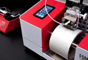
FOM Technologies is a leading provider in slot-die coating technology for new functional material.

Slot-die coating is a highly scalable technique for rapidly depositing thin and uniform films with minimal material waste and low operational cost. slot-die coating technology is used to deposit a variety of liquid chemistries onto substrates of various materials such as glass, metal, and polymers. This is achieved by precisely metering the process fluid; dispensing it at a controlled rate while the coating die is moved relative to the substrate.

FOM Technologies provides high-quality roll-based slot-die coating machines produced in Scandinavia. Our cutting-edge equipment enables researchers, scientists, and professionals, to discover, develop and commercialize new functional materials for a cleaner and more sustainable world. We strive hard to ensure that our products always are innovative, reliable, and cost-effective.

High-Quality Roll-Based Machines

Entry Level – FOM nanoRC – LinkThe FOM nanoRC is a lightweight, cost-efficient, easy to use, precision instrument for testing slot-die coating of solution-processable material onto flexible substrates.Intermediate Level – FOM arcRC – LinkOriginally designed for OPV and LEC research, the FOM arcRC is ideal for researchers who wish to work with flexible substrates or scale-up from spin coating.

Advanced Level – FOM moduloR2C – LinkThe FOM moduloR2C addresses the challenges associated with roll-to-roll equipment in R&D environments. Industrial roll-to-roll equipment often lacks the necessary freedom to experiment, adapt and data collect as is common in research.

High-Quality Sheet-Based Machines

Intermediate Level – FOM vectorSC – LinkThe system was designed for fast and easy coating of functional materials in laboratories working to develop novel materials, test device structures, and process devices for performance testing. It is intended for solution-processed thin-film coatings of functional materials, for example, related to solar (OPV, perovskites, CIGS), lighting, sensing, and energy storage applications.

Advanced Level – FOM alphaSC – Link

Industrial Level – FOM pontemSC – LinkThe FOM pontumSC provides an automated slot-die sheet coating system for high-end applications requiring high precision control of coating in repeated sheetfed steps.

Slot-die HeadsFOM Technologies state-of-the-art slot-die heads have been designed to provide outstanding coating properties and simple compatibility with FOM coating machines. Variable head sizes and viscosity ratings combined with flexible shim thickness and stripe pattern options provide access to a user-friendly, high-quality coating platform for a broad range of thin-film applications.Our Research Series contains comprehensive solutions for lab-scale applications, while our Industrial Series has been developed to support pilot-scale installations and beyond. Made from some of the hardest steel in the world, our slot-die heads are the product of a world-class manufacturing process, offering low dead volume, excellent flow properties, and treatment for robust chemical resistance. Following years of innovation and optimization, we are proud to offer slot-die heads that meet the needs of professional materials researchers above all else.

Link: https://www.fomtechnologies.com/products#slotdie​​​​